A 300mm Wafer Backside Review SEM solution that preserves the wafer while connecting backside defect review with SEM imaging, EDS elemental analysis, reporting, and process feedback.
Designed around 300mm wafer backside review use cases.
Non-destructiveBackside Review
Supports defect review while preserving the wafer without sample cutting.
150 points/waferReview Basis
Structured for multi-point analysis workflows and expanded review coverage.
TAT 160xReduction Target
Targets faster in-fab feedback compared with conventional out-fab destructive analysis.
100xAnalysis Volume Target
Aims to expand analysis points through repeatable review and automation linkage.
SEM + EDSImaging and Elemental Analysis
Connects SEM observations and elemental information to process feedback.
Evaluation Highlights
Damage Free Backside Review
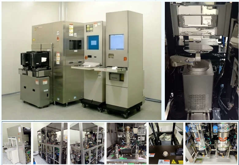
Public-facing equipment and analysis images from the presentation materials have been reorganized for the product page.
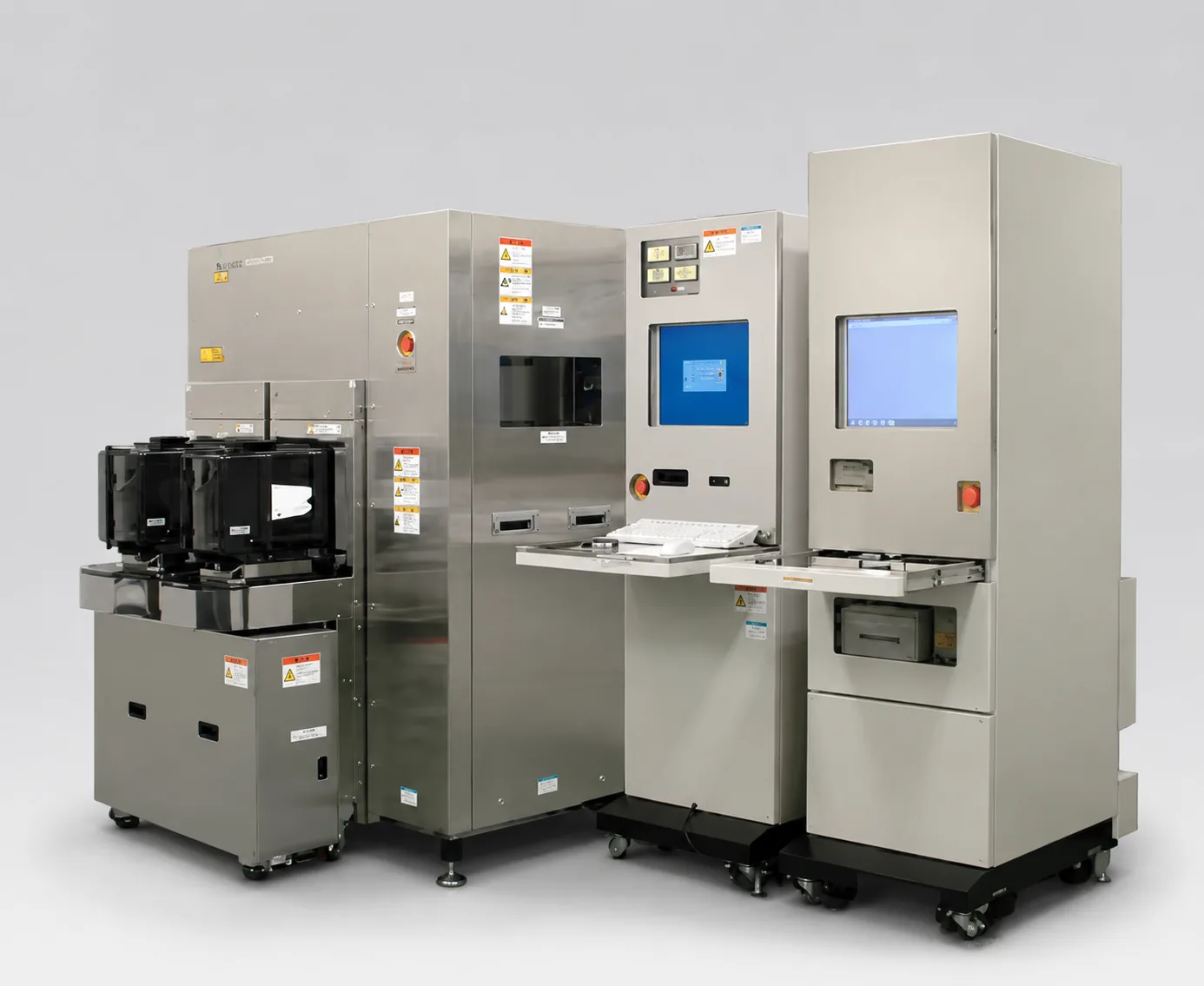
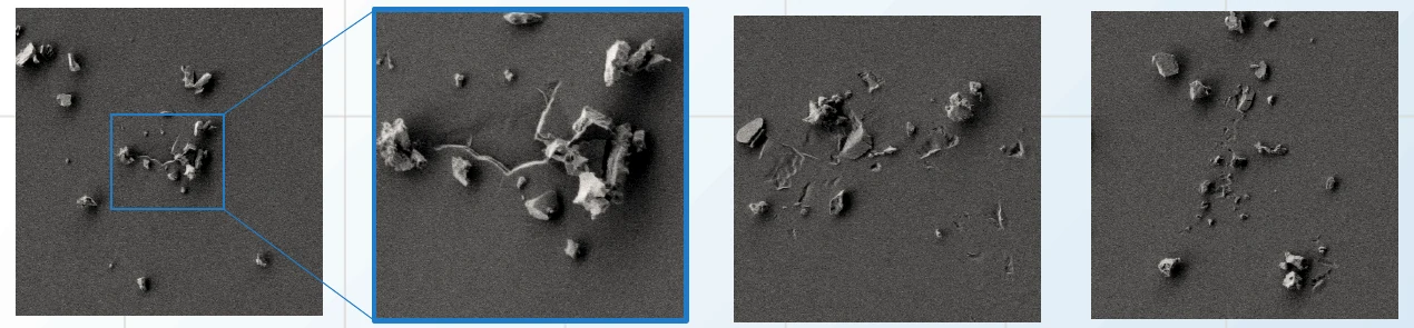
Sample SEM Review ImageExplains a workflow for reviewing backside particles and surface issues based on defect coordinates identified by optical inspection.Equipment / Handling ModuleExample equipment configuration for backside observation holders and damage-free review conditions.
Dedicated Wafer Backside Holder
Dedicated holder and observation conditions are reviewed to reduce wafer surface damage during backside review.
Low-Voltage Observation
Operating conditions including sub-1kV observation are reviewed to minimize beam damage and secure charge-less conditions.
Defect Navigation
SEM review positions can be aligned using defect coordinates detected by optical inspection tools.
SEM / EDS Linkage
Shape observation and elemental analysis are combined to support review of particles, contamination, and process abnormalities.
Features
BSR-1000 Features
Non-destructive Backside Review
Complements destructive failure analysis by enabling in-fab review of backside defects while preserving the wafer.
SEM / EDS Analysis
Provides evidence for defect root-cause review by combining morphology and elemental information.
Automation & Report
Recipe operation, ADR/ADC linkage, data upload, and report generation are reviewed according to customer operation scenarios.
Specifications
BSR-1000 Specifications
Detailed specifications will be updated after confirmation. Actual specifications and throughput may vary by process, sample, and automation scope.
Product Type300mm Wafer Backside Review SEM
ApplicationWafer backside defect review, failure analysis, process abnormality feedback
Analysis MethodNon-destructive SEM review with EDS elemental analysis support
Wafer / SampleFocused on 300mm wafer applications; details to be confirmed by process condition
NavigationDefect navigation based on optical inspection coordinates