技術
Technology insight from SEM principles to process applications
SEM scans a sample surface with an electron beam in vacuum and converts signals generated by electron-sample interaction into images and analytical data. HiKM connects this principle to tool selection, defect review, metrology, and maintenance decisions.
SEM uses electrons and electromagnetic lenses instead of light and glass lenses. It observes surface microstructures at high magnification in vacuum rather than in air.
TEM mainly uses transmitted electron information, while SEM uses signals generated from the sample surface such as secondary and backscattered electrons.
With deep depth of focus, rich surface information, and signal selectivity, SEM supports CD measurement, defect review, elemental analysis, and process feedback.
SEM Comparison
光学顕微鏡とSEMの違い
検査目的と必要分解能に応じて選定基準は異なります。SEMは電子ビーム観察を用いるため、高倍率・高分解能の表面分析に適しています。
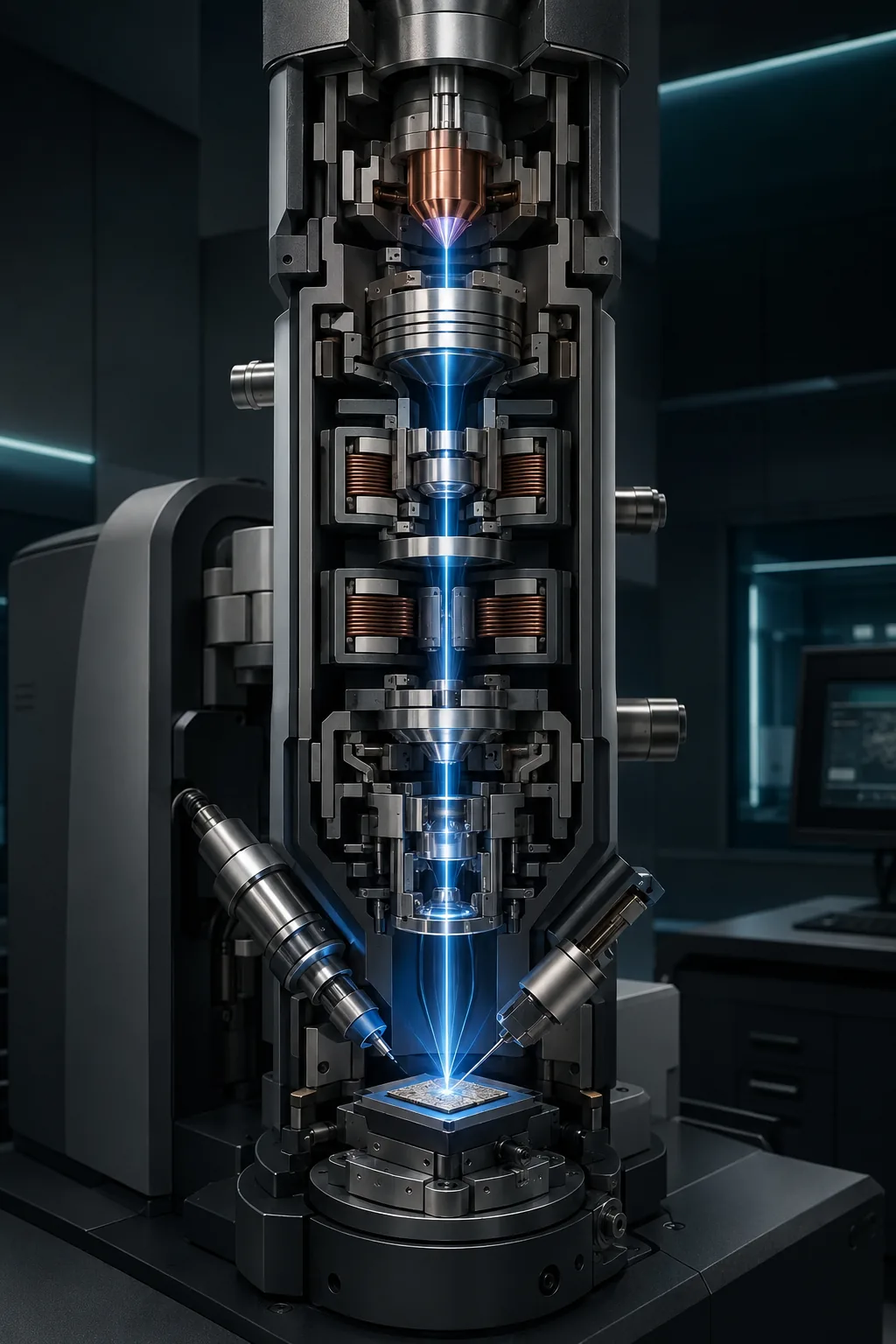
How an SEM system creates an image
The electron beam generated by the electron gun is reduced into a small probe through condenser and objective lenses. Scan coils move the probe across X-Y positions on the sample surface, and detectors convert the signal intensity at each position into image brightness and contrast.
- Electron gun: stable electron emission and beam current generation
- Electron lenses: control of probe size, resolution, and focus conditions
- Vacuum system: reduces electron scattering and sample contamination
- Detectors: collect SE, BSE, and X-ray signals for each observation goal
Signal Strategy
SEM signals to select by observation goal
This section organizes electron-solid interaction, SEM overview, optical microscope vs. SEM comparison, and SEM analysis characteristics in a way technical buyers can understand quickly.
Clarify whether the goal is CD measurement, defect review, elemental analysis, or surface observation.
Tune acceleration voltage, probe current, working distance, and detector choice for the sample and analysis goal.
Connect recipes, repeat inspection, ADR/ADC/EDS, data upload, and maintenance into the operating workflow.
SEM Comparison Detail
光学顕微鏡とSEMの主要比較基準
検査目的と必要分解能に応じて装置選定基準が変わるため、光源・分解能・倍率・運用環境をあわせて確認します。